Semiconductor Manufacturing Cost Calculator
How This Works
Estimate costs based on industry-standard data from the article. Inputs reflect real-world semiconductor manufacturing parameters.
Build Cost: $0
Monthly Operations: $0
Time to Fabricate One Batch: 0 weeks
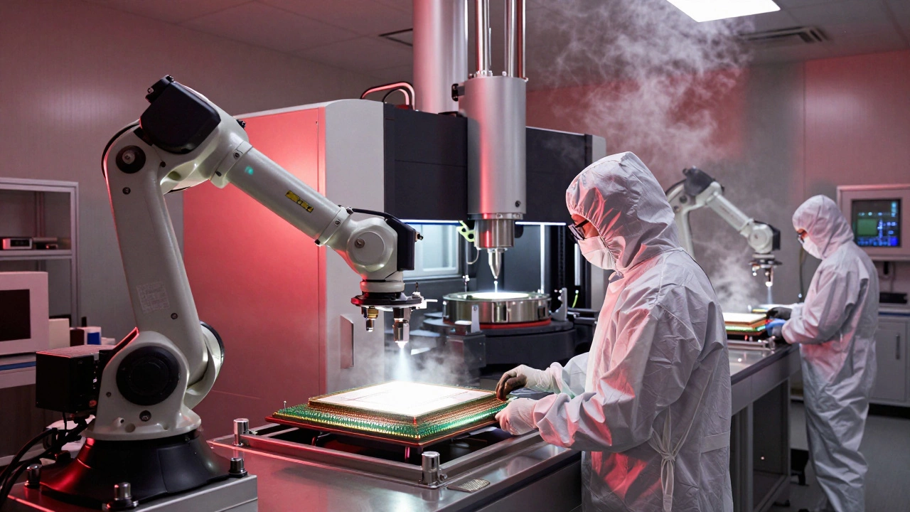
There’s no single manufacturing process that wins the title of "most complex" by brute force. But if you look at precision, scale, cost, and the sheer number of variables that must stay perfect for months on end, one process stands out: semiconductor fabrication. This isn’t just making chips. It’s building microscopic computers inside clean rooms where even a single speck of dust can ruin a billion-dollar batch.
Why Semiconductor Fabrication Is the Hardest
Think about this: a single smartphone chip has over 20 billion transistors. Each one is smaller than a virus. To make them, you need to etch patterns thinner than a human hair onto a silicon wafer-over 500 times. And you do it in layers, one on top of the other, with each layer needing perfect alignment. A misalignment of 10 nanometers? The chip fails.
The process takes 12 to 16 weeks. During that time, the wafer passes through 1,000+ steps. Each step requires a different machine, a different chemical, a different temperature, and a different gas. One machine alone-the extreme ultraviolet (EUV) lithography system-costs $150 million. It uses mirrors the size of small cars to bounce light at 13.5 nanometers wavelength to carve patterns. That light comes from a plasma of tin droplets fired at 50,000 times per second. If one droplet misses, the pattern is flawed.
And it’s not just the machines. The air in the clean room has fewer than 10 particles per cubic foot. Workers wear full-body suits that look like astronauts. Even breathing too close to the wafer can contaminate it. The water used to rinse the wafers is purified to 18 megohm-cm resistance-pure enough to dissolve your skin if you touched it. And the chemicals? Some are so reactive they explode on contact with air.
How It Compares to Other "Complex" Processes
People mention pharmaceuticals, aerospace engines, or nuclear reactors as complex. And they are. But they’re complex in different ways.
Pharmaceutical manufacturing needs strict regulatory control. One wrong ingredient in a batch of insulin can kill. But the process itself? It’s mostly mixing, heating, filtering. It’s precise, yes-but not at the atomic scale.
Aerospace turbines are made from single-crystal nickel alloys, shaped with laser precision. They must survive 1,700°C and 100 times Earth’s gravity. But you only make a few hundred per year. Semiconductor fabs produce billions of chips annually.
Steel manufacturing? It’s heavy, hot, and loud. But the chemistry is well understood. You melt iron, add carbon, cool it. Repeat. Semiconductor fabrication is like trying to build a working city inside a snowflake-while the snowflake is still falling.
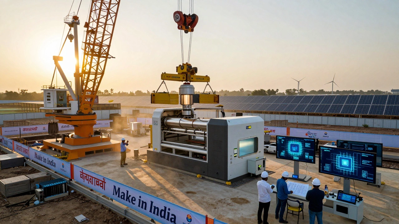
The Role of Government Schemes
Because this process is so hard, so expensive, and so critical, governments around the world are stepping in. The U.S. CHIPS Act, the EU Chips Act, India’s Production Linked Incentive (PLI) scheme, and China’s "Made in China 2025" all pour billions into building domestic chip-making capacity.
Why? Because the world runs on chips. Your car, your fridge, your phone, your hospital equipment-they all need them. When supply chains broke during the pandemic, entire industries shut down. A single factory in Taiwan or South Korea can control 90% of the world’s most advanced chips. That’s not just an economic risk. It’s a national security risk.
Government schemes don’t just give money. They fund research into next-gen materials like gallium nitride, build training programs for nanotechnology engineers, and create tax breaks for companies that bring fabs onshore. In the U.S., the government is funding $52 billion in direct grants. In India, companies get up to 25% of their capital investment back as a subsidy.
But here’s the catch: even with billions in funding, building a new chip factory takes 3 to 5 years. And you need 2,000+ skilled workers-engineers, technicians, chemists-just to run it. There aren’t enough trained people. That’s why governments are now partnering with universities to create specialized degrees in semiconductor science.

The Human Side of Complexity
Behind every chip is a team of people who’ve spent decades mastering this craft. A process engineer might spend 10 years learning how to tweak a single step in the etching sequence. A metrology specialist uses electron microscopes to inspect features smaller than a wavelength of light. They don’t just fix machines-they predict how a machine will fail before it breaks.
There’s no room for error. One mistake in a single step can cost $50 million in lost wafers. That’s why every shift starts with a 45-minute safety and quality review. Every tool is calibrated daily. Every chemical batch is tested three times.
And yet, the pace never slows. Moore’s Law may be slowing, but demand isn’t. AI chips need more transistors. Electric vehicles need more power control chips. Drones, robots, smart cities-all need more silicon. So the pressure keeps building.
What’s Next? The Next Level of Complexity
Right now, the industry is moving toward 3D chip stacking. Instead of making transistors flat on a wafer, they’re stacking them like floors in a skyscraper. This means connecting transistors vertically with tiny copper pillars thinner than a human hair. It’s called chiplet architecture. It’s the future.
But it’s even harder. Aligning layers vertically? That’s a new kind of precision. Thermal expansion mismatches between layers can crack the chip. Testing each layer after stacking? That’s a whole new challenge.
Meanwhile, researchers are experimenting with quantum dots, carbon nanotubes, and photonic chips. These aren’t just improvements-they’re entirely new ways of computing. But they’re still in labs. None have scaled to mass production.
For now, silicon and EUV lithography remain king. And they’re still the most complex manufacturing process ever created by humans.
Why This Matters to Everyone
You don’t need to understand how a chip is made to use your phone. But you should know that the thing you hold in your hand is the result of the most intricate, expensive, and fragile manufacturing system on Earth. If that system breaks-because of war, a natural disaster, or a supply chain failure-your car won’t start. Your hospital might lose diagnostic tools. Your online bank might go down.
That’s why governments are investing billions. Not because they love chips. But because they know: the future runs on silicon. And no one else can make it like this.
Is semiconductor fabrication the most expensive manufacturing process?
Yes. A single advanced semiconductor fabrication plant (fab) costs $10 billion to $20 billion to build. That’s more than an aircraft carrier. The EUV lithography machine alone costs $150 million. Operating costs are equally high-power, ultra-pure water, specialty gases, and cleanroom maintenance run over $1 million per day. No other manufacturing process comes close in upfront or ongoing cost.
Why can’t other countries easily copy chip-making technology?
It’s not just about buying machines. The real knowledge is in the process recipes-exact chemical mixtures, timing, temperatures, and sequences developed over decades. These are trade secrets, guarded fiercely. Even if you get a machine, without the right software, calibration, and trained engineers, you can’t make a working chip. It’s like having a Ferrari but no driver’s license or road map.
How long does it take to make a single chip?
From raw silicon wafer to finished chip, the process takes 12 to 16 weeks. That’s over three months. During that time, the wafer goes through more than 500 steps-deposition, lithography, etching, implantation, cleaning, testing. Each step must be flawless. Any mistake means the entire batch could be scrapped.
What’s the role of government in semiconductor manufacturing?
Governments fund the construction of fabs, subsidize R&D, train engineers, and create tax incentives. Because private companies alone can’t afford the risk, public investment is essential. The U.S. CHIPS Act, EU Chips Act, and India’s PLI scheme are all trying to reduce dependence on a few global suppliers-mainly in Taiwan and South Korea.
Can 3D chip stacking replace traditional chip manufacturing?
No-not yet. 3D stacking (chiplets) is an evolution, not a replacement. It still relies on the same foundational processes: lithography, etching, deposition. It just layers them vertically. The challenge now is connecting layers without overheating or cracking. It’s harder than making flat chips, but it’s built on the same complex system.
What You Can Do to Understand This Better
If you’re curious, start by watching short videos from Intel, TSMC, or ASML. They show real footage inside clean rooms. You’ll see robots moving wafers under red lights, lasers firing, and technicians in bunny suits. It looks like science fiction-but it’s real, happening right now.
Follow news on government funding. When the U.S. or India announces a new chip plant, that’s not just a factory-it’s the future being built, one nanometer at a time.